
[Edit of Image1]
Introduction
Hey it's a me again @drifter1!
Today we continue with the Logic Design series on Verilog to get into a Combinational Logic Testbench Example.
So, without further ado, let's get straight into it!
Half Adder
Let's start off with the simplest form of an addition circuit, the so called Half Adder.
An Half Adder takes two 1-bit inputs A and B, and outputs a 1-bit sum (S) and a 1-bit carry (C). When either of the two inputs is 0 the sum and carry are also zero. When only one of the two inputs is 1 then the sum is 1 and the carry is 0. Lastly, if both inputs are 1, then the sum is 0 and the carry is 1.
Thus, the Truth Table is:
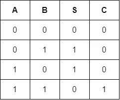
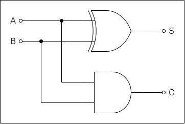
It's easy to see that the output S, which is the sum, follows the XOR logic pattern, whilst the output C, which is the carry, follows the AND logic pattern. In other words, an Half Adder is basically the following logic circuit:
Implementation
Implementing such a simple circuit is a piece of cake in Verilog. Let's use gate primitives for this implementation, which allows us to instantiate built-in Verilog modules that implement the fundamental logic circuits. As always, outputs have to be defined and mapped before the inputs in these instantiations. Because all of the inputs and outputs are 1-bit wires there is also no need to specify the wire data type or the bit length, a simple input and output keyword are sufficient.
An half adder is thus:
module half_adder (output s, c, input a, b);
    xor (s, a, b);
    and (c, a, b);
endmodule
Testbench
A testbench for this simple circuit is easy to implement. From the previous part of the series we know that a testbench doesn't have any I/O, and that the inputs are defined as reg types, whilst the outputs are defined as wire types. Let's also map the ports directly, using positional mapping.
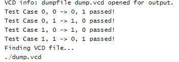
Of course, there are only four test cases. So, let's define one initial block which will give the corresponding inputs, wait for one simulation cycle, and keep going. After each test case, let's add a conditional statement, which checks the outputs and prints a message to the console using the $display system task.
Let's not forget to include the $dumpfile and $dumpvars system tasks, which are used in simulations, and after the testing is done, let's also use the $finish system task to terminate the simulation. For the timescale, let's use 1ns / 1ps.
The Verilog HDL code for all that is simply:
`timescale 1ns/1ps

module half_adder_tb;
    reg a, b;
    wire s, c;

    half_adder UUT (s, c, a, b);

    initial begin
        $dumpfile("dump.vcd");
        $dumpvars;

        // test case 0, 0 -> 0, 0
        a = 0;
        b = 0;
        #1;

        if ((s == 0) && (c == 0))
            $display("Test Case 0, 0 -> 0, 1 passed!");
        else
            $display("Test Case 0, 0 -> 0, 1 failed!");

        // test case 0, 1 -> 1, 0
        a = 0;
        b = 1;
        #1;

        if ((s == 1) && (c == 0))
            $display("Test Case 0, 1 -> 1, 0 passed!");
        else
            $display("Test Case 0, 1 -> 1, 0 failed!");

        // test case 1, 0 -> 1, 0
        a = 1;
        b = 0;
        #1;

        if ((s == 1) && (c == 0))
            $display("Test Case 1, 0 -> 1, 0 passed!");
        else
            $display("Test Case 1, 0 -> 1, 0 failed!");

        // test case 1, 1 -> 0, 1
        a = 1;
        b = 1;
        #1;

        if ((s == 0) && (c == 1))
            $display("Test Case 1, 1 -> 0, 1 passed!");
        else
            $display("Test Case 1, 1 -> 0, 1 failed!");

        $finish;
    end
endmodule
Simulation using EDA Playground
Let's use EDA Playground in order to simulate this circuit.
After logging in, just paste in the corresponding Verilog codes, as shown below:

In order to avoid simulation problems, we also include the same timescale in the right module.
In the left menu, we choose Icarus Verilog 0.9.7 as the compilation tool and tick the Open EPWave after run box.

After that we simply hit the Run button in the top menu.

Doing that, the corresponding wave form pops up.

And closing that window, we can also see the console print out the passed messages as well.
Simulation using ModelSim
Simulation using the ModelSim software is also quite straightforward. I will skip the installation procedure, so let's get into the basic steps of simulation.
From the toolbar open the directory where the Verilog modules are located.
In the console type vlib work followed by vmap work work in order to initialize the work space.

Compile the two Verilog modules by typing:
vlog half_adder.v
vlog half_adder_tb.v
Afterwards, simulate the testbench, add all the signals and simulate the complete testbench by typing:
vsim half_adder_tb
add wave *
run -all
The following waveform pops up:

And the console prints out:

Let's note, that $finish was replaced by $stop, cause else the complete software shuts down (after a message box though).
Note: In small designs the waveforms are mostly sufficient! But in more complicated designs getting less output, which for example tells if all the test cases passed successfully, or which cases failed, might be far more useful. This takes time to master, so don't worry too much about it!
RESOURCES:
References
- http://www.asic-world.com/verilog/veritut.html
- https://www.chipverify.com/verilog/verilog-tutorial
- https://www.javatpoint.com/verilog
Images
Block diagrams and other visualizations were made using draw.io
Previous articles of the series
- Introduction → Basic Syntax, Data Types, Operators, Modules
- Combinational Logic → Assign Statement, Always Block, Control Blocks, Gate-Level Modeling and Primitives, User-Defined Primitives
- Combinational Logic Examples → One Circuit - Four Implementations, Encoder, Decoder, Multiplexer
- Sequential Logic → Procedural Blocks (Initial, Always), Blocking and Non-Blocking Assignments, Statement Groups
- Sequential Logic Examples → Flip Flops (DFF, TFF, JKFF, SRFF), N-bit Counter, Single-Port RAM
- Finite-State Machines → Finite-State Machine (FSM), FSM Types, State Encoding, Modeling FSMs in Verilog
- Finite-State Machine Examples → Moore FSM Example (1 and 2 always blocks), Mealy FSM Example (1, 2 and 3 always blocks)
- Testbenches and Simulation → Testbenches (DUT / UUT, Syntax, Test Cases), System Tasks, Simulation Tools
Final words | Next up
And this is actually it for today's post!
Next time we will get into a Sequential Logic Testbench, which will basically be a simple FSM...
See Ya!

Keep on drifting!